(Hong Kong)


Product Summary
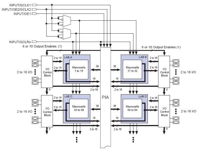
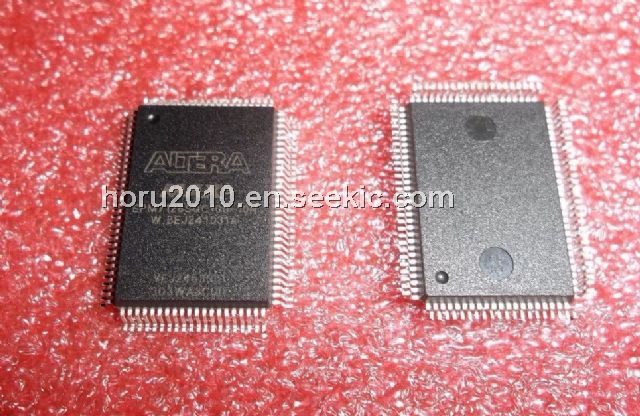
The EPM712SQC100-10 is a Programmable Logic Device. The EPM712SQC100-10 includes four dedicated inputs that can be used as general-purpose inputs or as high-speed, global control signals (clock, clear, and two output enable signals) for each macrocell and I/O pin. Figure 1 shows the architecture of MAX 7000A devices.
Parametrics
EPM712SQC100-10 absolute maximum ratings: (1)VCC Supply voltage With respect to ground (2): –0.5 to 4.6 V; (2)VI DC input voltage: –2.0 to 5.75 V; (3)IOUT DC output current, per pin: –25 to 25 mA; (4)TSTG Storage temperature No bias: –65 to 150℃; (5)TA Ambient temperature Under bias: –65 to 135℃; (6)TJ Junction temperature BGA, FineLine BGA, PQFP, and TQFP packages, under bias: 135℃.
Features
EPM712SQC100-10 features: (1)High-performance 3.3-V EEPROM-based programmable logic devices (PLDs) built on second-generation Multiple Array MatriX (MAXR) architecture (see Table 1); (2)3.3-V in-system programmability (ISP) through the built-in IEEE Std. 1149.1 Joint Test Action Group (JTAG) interface with advanced pin-locking capability; (3)MAX 7000AE device in-system programmability (ISP) circuitry compliant with IEEE Std. 1532; (4)EPM7128A and EPM7256A device ISP circuitry compatible with IEEE Std. 1532; (5)Built-in boundary-scan test (BST) circuitry compliant with IEEE Std. 1149.1; (6)Supports JEDEC Jam Standard Test and Programming Language (STAPL) JESD-71; (7)Enhanced ISP features; (8)Enhanced ISP algorithm for faster programming (excluding EPM7128A and EPM7256A devices); (9)ISP_Done bit to ensure complete programming (excluding EPM7128A and EPM7256A devices); (10)Pull-up resistor on I/O pins during in-system programming; (11)Pin-compatible with the popular 5.0-V MAX 7000S devices; (12)High-density PLDs ranging from 600 to 10,000 usable gates; (13)Extended temperature range.
Diagrams