(Hong Kong)

Product Summary
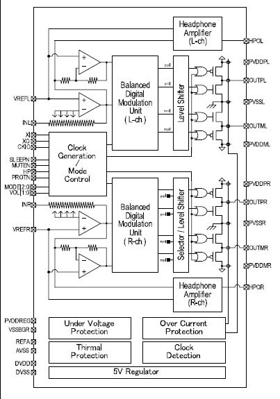
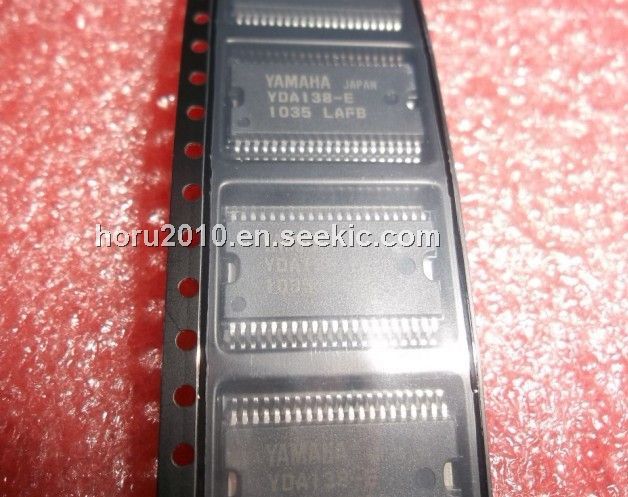
The YDA138-E is a high efficient digital audio power amplifier IC that operates with a single 12V power supply. An audio power amplifier with a maximum output of 10W (RL=8Ω)×2ch or 20W (RL=4Ω)×1ch can be configured with one chip. The YDA138-E has a “Pure Pulse Direct Speaker Drive Circuit” which directly drives speakers while reducing distortion of pulse output signal and reducing noise on the signal, and realizes the highest standard low distortion rate characteristics and low noise characteristics as 10W-class of output digital amplifier IC.
Parametrics
YDA138-E absolute maximum ratings: (1)Power supply terminal (VDDP) Voltage Range Note 1,2,3) VDDP: -0.3 to 14.0 V; (2)SLEEPN, PROTN terminal Voltage Range VIN1: VSS-0.3 to VDDP+0.3 V; (3)CKIO Input/Output terminal Voltage Range VIN2: VSS-0.3 to VREG+1.0 V; (4)Voltage Range of terminals for control Note 4) VIN3: VSS-0.3 to VREG+1.0 V; (5)Voltage Range of Input/output terminals Note 5) VIN4: VSS-0.3 to VREG+0.3 V; (6)Allowable dissipation (Ta=25℃) PD25: 2.7 W; (7)Allowable dissipation (Ta=70℃) PD70: 1.45 W; (8)Junction temperature TJMAX: 125℃; (9)Storage Temperature TSTG: -50 to 125℃.
Features
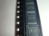
YDA138-E features: (1)Operating power supply range 9.0V to 13.5V; (2)Multi-channel synchronizing operation by Master/Slave switching function; (3)Carrier frequency switching function 524kHz/466kHz; (4)Sleep function with SLEEPN terminal; (5)Output muting function with MUTEN terminal; (6)Over-current protection function; (7)Thermal protection function; (8)Clock stop detection function; (9)Pop noise reduction function; (10)AM interference measures function; (11)Analog input/BTL (Bridge-Tied Load) output; (12)42-pin plastic SSOP Pin lead plating with Pd free (YDA138-EZ).
Diagrams