(Hong Kong)

Product Summary
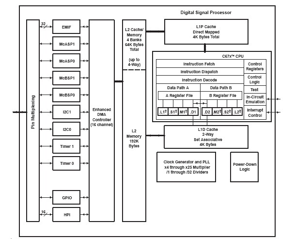
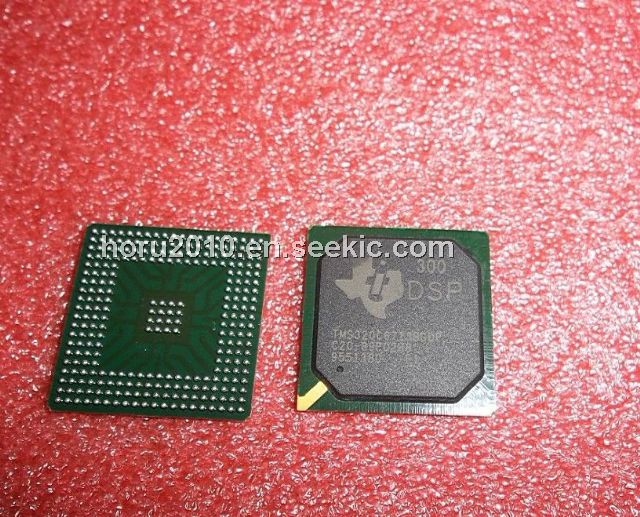
The TMS320C6713BGDPC20 is a floating-point digital signal processor. The TMS320C6713BGDPC20 uses a two-level cache-based architecture and has a powerful and diverse set of peripherals. The Level 1 program cache (L1P) is a 4K-byte direct-mapped cache and the Level 1 data cache (L1D) is a 4K-byte 2-way set-associative cache. The Level 2 memory/cache (L2) consists of a 256K-byte memory space that is shared between program and data space. 64K bytes of the 256K bytes in L2 memory can be configured as mapped memory, cache, or combinations of the two. The remaining 192K bytes in L2 serves as mapped SRAM. The TMS320C6713BGDPC20 has a rich peripheral set that includes two Multichannel Audio Serial Ports (McASPs), two Multichannel Buffered Serial Ports (McBSPs), two Inter-Integrated Circuit (I2C) buses, one dedicated General-Purpose Input/Output (GPIO) module, two general-purpose timers, a host-port interface (HPI), and a glueless external memory interface (EMIF) capable of interfacing to SDRAM, SBSRAM, and asynchronous peripherals.
Parametrics
TMS320C6713BGDPC20 absolute maximum ratings: (1)Supply voltage range, CVDD (see Note 2): -0.3 V to 1.8 V; (2)Supply voltage range, DVDD (see Note 2): -0.3 V to 4 V; (3)Input voltage range : -0.3 V to DVDD + 0.5 V; (4)Output voltage range: -0.3 V to DVDD + 0.5 V; (5)Operating case temperature ranges, TC: (default): 0 to 90℃; (6)(A version) [GDPA/ZDPA-200, PYPA-167,-200]: -40℃ to 105℃; (7)Storage temperature range, Tstg: -65℃ to 150℃.
Features
TMS320C6713BGDPC20 features: (1)Highest-Performance Floating-Point Digital Signal Processor (DSP): TMS320C6713B; (2)Advanced Very Long Instruction Word (VLIW) TMS320C67x. DSP Core; (3)L1/L2 Memory Architecture; (4)32-Bit External Memory Interface (EMIF); (5)Enhanced Direct-Memory-Access (EDMA) Controller (16 Independent Channels); (6)16-Bit Host-Port Interface (HPI); (7)Two 32-Bit General-Purpose Timers; (8)Dedicated GPIO Module With 16 pins (External Interrupt Capable); (9)Flexible Phase-Locked-Loop (PLL) Based Clock Generator Module; (10)IEEE-1149.1 (JTAG) Boundary-Scan-Compatible; (11)208-Pin Power PAD PQFP (PYP); (12)272-BGA Packages (GDP and ZDP); (13)0.13-μm/6-Level Copper Metal Process CMOS Technology; (14) 3.3-V I/Os, 1.4V Internal (GDP/ZDP) [300 MHz].
Diagrams