(Hong Kong)

Product Summary
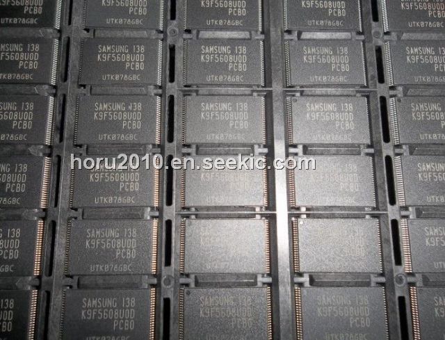
The K9F5608U0D-PCB0 is a 32M x 8 Bit NAND Flash Memory. The K9F5608U0D-PCB0 is Offered in 32M × 8bit, the K9F5608U0D-PCB0 is 256M bit with spare 8M bit capacity. The K9F5608U0D-PCB0 is offered in 1.8V, 2.65V, 3.3V Vcc. The K9F5608U0D-PCB0’s NAND cell provides the most cost-effective solutIon for the solid state mass storage market. A program operation of the K9F5608U0D-PCB0 can be performed in typical 200μs on a 528-byte page and an erase operation can be performed in typical 2ms on a 16K-byte block. Data in the page can be read out at 50ns cycle time per byte. The I/O pins serve as the ports for address and data input / output as well as command input. The on-chip write control of the K9F5608U0D-PCB0 automates all program and erase functions including pulse repetition, where required, and internal verification and margining of data. Even the write-intensive systems can take advantage of the K9F5608U0D-PCB0’s extended reliability of 100K program/erase cycles by providing ECC(Error Correcting Code) with real time mapping-out algorithm.
Parametrics
K9F5608U0D-PCB0 absolute maximum ratings: (1)Voltage on any pin relative to VSS, VIN/OUT: -0.6 to + 4.6 V; (2)Temperature Under Bias, TBIAS: -10 to +125 ℃; (3)Storage Temperature, TSTG: -65 to +150 ℃; (4)Short Circuit Current, Ios: 5 mA.
Features
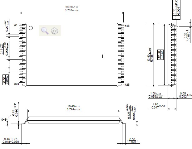
K9F5608U0D-PCB0 features: (1)Voltage Supply: 2.7 to 3.6 V; (2)Organization: Memory Cell Array; (3)Automatic Program and Erase: Page Program; (4)Page Read Operation: Page Size; (5)Fast Write Cycle Time, Program time: 200μs; (6)Command/Address/Data Multiplexed I/O Port; (7)Hardware Data Protection; (8)Reliable CMOS Floating-Gate Technology; (9)Command Register Operation; (10)Intelligent Copy-Back; (11)Unique ID for Copyright Protection; (12)Package: 48 - Pin WSOPI.
Diagrams