(Hong Kong)

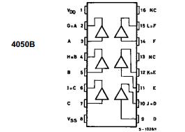
Product Summary
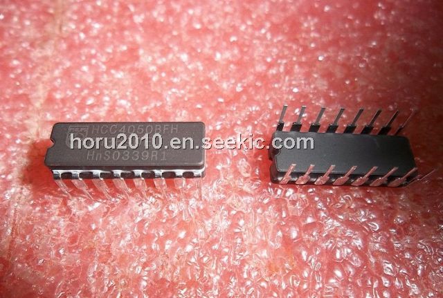
The HCC4050BFH is a Hex buffer/converter. The HCC4050BFH is a monolithic integrated circuit available in 16-lead dual in-line plastic or ceramic package and plastic micropackage. The HCC4050BFH is a inverting and non-inverting hex buffer, respectively, and features logic-level conversion using only one supply voltage (VDD) .
Parametrics
HCC4050BFH absolute maximum ratings: (1) Supply Voltage VDD: -0.5 to +20V; (2) Input Voltage Vi: -0.5 to VDD +0.5V; (3) DC Input Current(anyone input) : ±10mA; (4) Total Power Dissipation (per package) : 200mW; (5) Dissipation per Output Transistor for Top=FulPackage-temperature Range: 100mW; (6) Operating Temperature Top: -55 to +125°C; (7) Storage Temperature Tstg: -65 to +150°C.
Features
HCC4050BFH features: (1) high sink current for driving 2 TTL loads; (2) high-to-low level logic conversion; (3) quiescent current specified to 20V for HCC device; (4) high SINK and SOURCE current capability; (5) 5V, 10V and 15V parametric ratings; (6) input current of 100nA and 25°C for HCC device; (7) 100% tested for quiescent current; (8) meets all requirements of JEDEC tentative standard 13A.
Diagrams