Product Summary
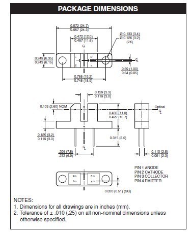
The H21B2 transmissive sensor consists of a gallium arsenide infrared emitting diode coupled with a silicon photodarlington in a plastic housing. The packaging system of H21B2 is designed to optimize the mechanical resolution, coupling efficiency, ambient light rejection, cost and reliability. The gap in the housing provides a means of interrupting the signal with an opaque material, switching the output from an “ON” to an “OFF” state.
Parametrics
H21B2 absolute maximum ratings: (1)Operating Temperature, TOPR: -55 to +100℃; (2)Storage Temperature, TSTG: -55 to +100℃; (3)Soldering Temperature (Iron) (2,3 and 4), TSOL-I: 240 for 5 sec℃; (4)Soldering Temperature (Flow) (2 and 3), TSOL-F: 260 for 10 sec℃; (5)Continuous Forward Current, IF: 50 mA; (6)Reverse Voltage, VR: 6V; (7)Power Dissipation, PD: 100 mW; (8)Collector to Emitter Voltage, VCEO: 30V; (9)Emitter to Collector Voltage, VECO: 6V; (10)Collector Current, IC: 40mA; (11)Power Dissipation (TC= 25℃), PD: 150mW.
Features
H21B2 features: (1)Opaque housing; (2)Low cost; (3)035" apertures; (4)High IC(ON).
Diagrams

| Image | Part No | Mfg | Description |  |
Pricing (USD) |
Quantity | ||||
|---|---|---|---|---|---|---|---|---|---|---|
 |
 H21B2_Q |
 Fairchild Semiconductor |
 Optical Switches, Transmissive, with Phototransistor Output INTERUP MOD DARL |
 Data Sheet |
 Negotiable |
|
||||
 |
 H21B2 |
 Fairchild Semiconductor |
 Optical Switches, Transmissive, with Phototransistor Output INTERUP MOD DARL |
 Data Sheet |
 Negotiable |
|
||||
 (Hong Kong)


