(Hong Kong)

Product Summary
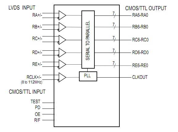
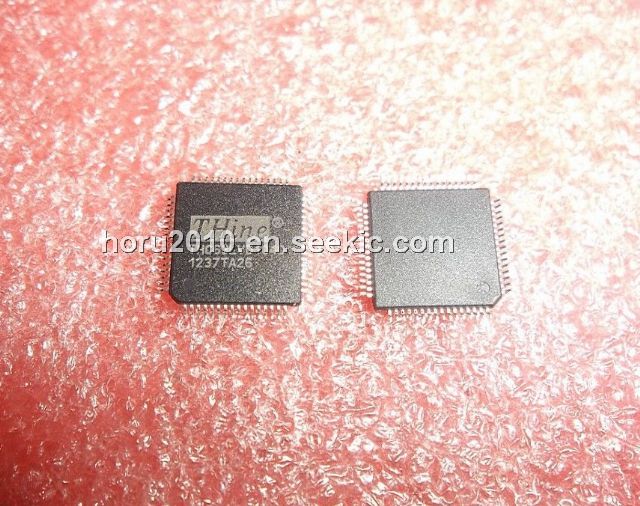
The THC63LVD104C is a COLOR LVDS Receiver. The THC63LVD104C is designed to support pixel data transmission between Host and Flat Panel Display from NTSC up to SXGA resolutions. The THC63LVD104C converts the LVDS data streams back into 35bits of CMOS/TTL data with the choice of the rising edge or falling edge clock for the convenience with a variety of LCD panel controllers. At a transmit clock frequency of 112MHz, 30bits of RGB data and 5bits of timing and control data (HSYNC, VSYNC, DE, CNTL1, CNTL2) are transmitted at an effective rate of 784Mbps per LVDS channel. Using a 112MHz clock, the data throughput of the THC63LVD104C is 490Mbytes per second.
Parametrics
THC63LVD104C absolute maximum ratings: (1)Supply Voltage (VCC=VCC=LVCC=PVCC): -0.3V to +4.0V; (2)CMOS/TTL Input Voltage: -0.3V to (VCC + 0.3V); (3)CMOS/TTL Output Voltage: -0.3V to (VCC + 0.3V); (4)LVDS Receiver Input Voltage: -0.3V to (VCC + 0.3V); (5)Output Current: -30mA to 30mA; (6)Junction Temperature: +125 ℃; (7)Storage Temperature Range: -55 to +150 ℃; (8)Reflow Peak Temperature / Time: +260 / 10 sec.; (9)Maximum Power Dissipation @+25 ℃: 2.1W.
Features
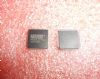
THC63LVD104C features: (1)Wide dot clock range: 8-112MHz suited for NTSC, VGA, SVGA, XGA, and SXGA; (2)PLL requires no external components; (3)50% output clock duty cycle; (4)TTL clock edge programmable; (5)Power down mode; (6)Low power single 3.3V CMOS design; (7)64pin TQFP; (8)Backward compatible with THC63LVDF64x (18bits) / F84x(24bits); (9)Pin compatible with THC63LVD104C; (10)Fail-safe for Open LVDS Input.
Diagrams