(Hong Kong)

Product Summary
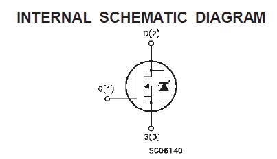
The STP11NB40 is an N-channel PowerMESH MOSFET. Using the latest high voltage MESH OVERLAY process, STMicroelectronics has designed an advanced family of power MOSFETs with outstanding performances. The new patent pending strip layout coupled with the Company’s proprietary edge termination structure, gives the lowest RDS(on) per area, exceptional avalanche and dv/dt capabilities and unrivalled gate charge and switching characteristics. The applications of the include high current, high speed switching, switch mode power supplies(smps), dc-ac converters for welding equipmentand uninterruptible powersupplies and motor drive.
Parametrics
STP11NB40 absolute maximum ratings: (1)VDS, Drain-source Voltage (VGS = 0): 400 V; (2)VDGR, Drain- gate Voltage (RGS = 20 kW): 400 V; (3)VGS, Gate-source Voltage: ±30 V; (4)ID, Drain Current (continuous) at Tc = 25℃: 10.7A; (5)ID, Drain Current (continuous) at Tc = 100℃: 6.7A; (6)IDM, Drain Current (pulsed):42.8 A; (7)Ptot, Total Dissipation at Tc = 25℃: 40 W; (8)Derating Factor: 1.0 W/℃; (9)dv/dt, Peak Diode Recovery voltage slope: 4.5 V/ns; (10)VISO, Insulat ion Withstand Voltage (DC): 2000 V; (11)Tstg, Storage Temperature: -65 to 150℃; (12)Tj, Max. Operating Junction Temperature: 150℃.
Features
STP11NB40 features: (1)typical rds(on) = 0.48 w; (2)extremely high dv/dt capability; (3)100% avalanche tested; (4)very low intrinsic capacitances; (5)gate charge minimized.
Diagrams
| Image | Part No | Mfg | Description |  |
Pricing (USD) |
Quantity | ||||||||||||
|---|---|---|---|---|---|---|---|---|---|---|---|---|---|---|---|---|---|---|
 |
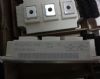
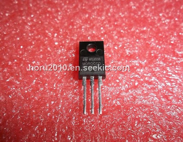
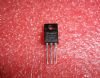
 STP11NB40 |
STMicroelectronics |
MOSFET N-Ch 400 Volt 11 Amp |
Data Sheet |
|
|
||||||||||||
|
STP11NB40FP |
Other |
|
Data Sheet |
Negotiable |
|
||||||||||||